Global Semiconductor Foundry Landscape: TSMC, Samsung, and Intel’s 2nm Node Strategy Update

Global Semiconductor Foundry Landscape- Visualization of the 2nm node race between TSMC, Samsung, and Intel strategies

1. Introduction: The Geopolitics and Physics of the 2-Nanometer Frontier   The semiconductor industry is entering the “Angstrom Era,” defined by the migration to 2nm-class process nodes (20A, 18A, N2). This transition is not merely an incremental step; it represents the largest architectural shift in transistor design since the move from planar transistors to FinFETs … Read more

2nm Chip War: How TSMC, Samsung, and Intel’s Battle Will Define Your Next iPhone’s Battery Life

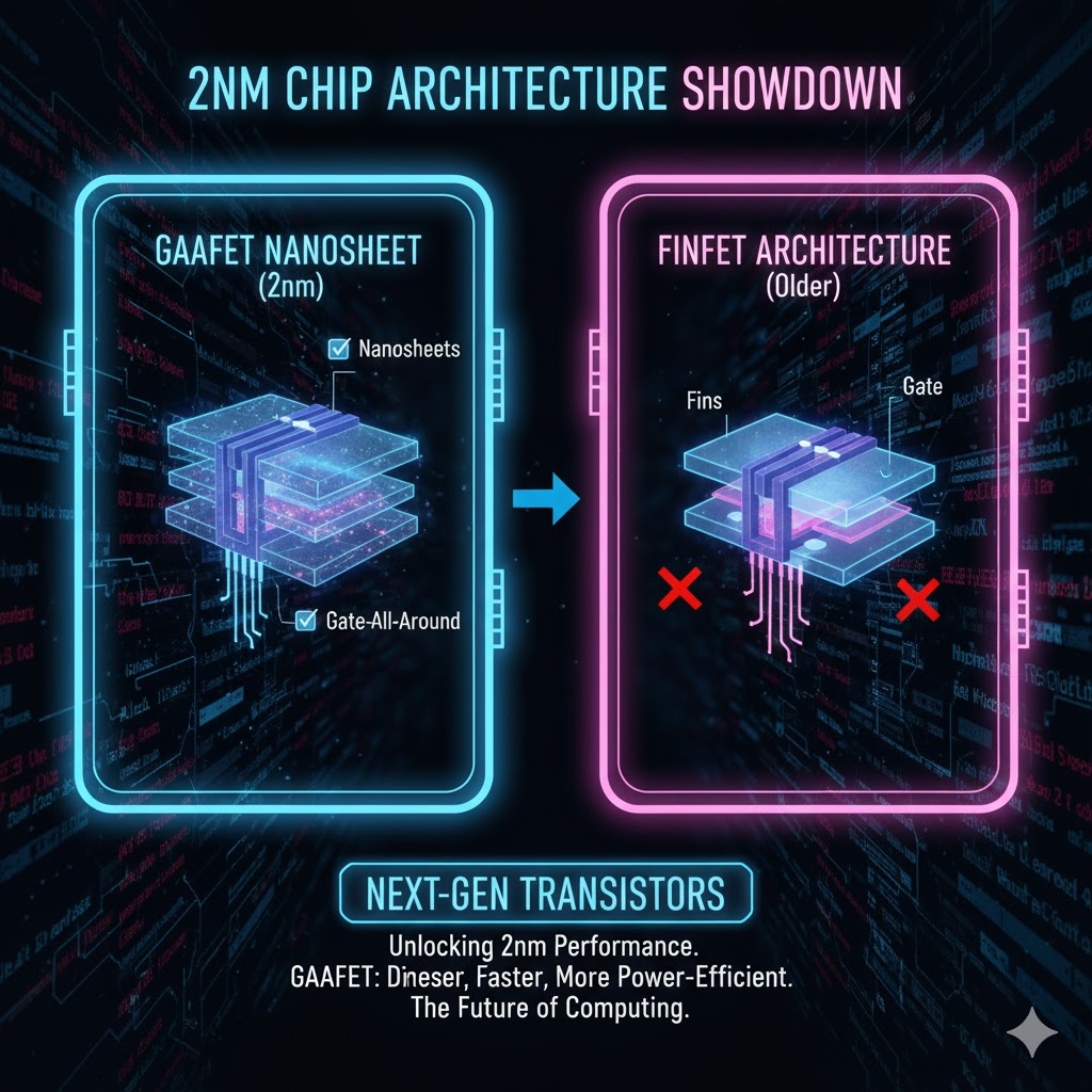
Diagram illustrating the Gate All Around GAAFET Nanosheet structure compared to the older FinFET architecture for 2nm chips

💡 The Angstrom Era The Foundry Triopoly at 2nm   The year 2026 marks the beginning of the Angstrom Era in semiconductor manufacturing, a period where critical dimensions are measured in tenths of a nanometer. This technological inflection point is defined by the shift from the venerable FinFET (Fin Field-Effect Transistor) architecture to the revolutionary … Read more